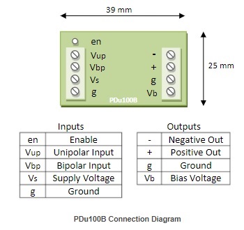
PDu100B Miniature Piezo Driver
Piezoelectric Drivers
 PDu100B Specifications
 Calculate Power Bandwidth
Specifications:
| PDu100B Specifications | |||
|---|---|---|---|
| Power Supply | 3 V to 5.5 V | ||
| Max. Unipolar Output | +60V | +90 V | +100 V |
| Max. Bipolar Output | +/-60 V | +/-90 V | +/- 100 V |
| RMS Output Current | 89 mA | 60mA | 33mA |
| Average DC Current | 40 mA | 18 mA | 15 mA |
| Power Bandwidth | 5.3 kHz | 3.5 kHz | 3.2 kHz |
| Peak Output Current | 100 mA | ||
| Signal Bandwidth | 60 kHz (unloaded) | ||
| Dimensions | 39 x 25 mm (1.5 x 1 in) | ||
| Weight | 5.5 g (0.2 oz) | ||
| Gain | 27.5 V/V | ||
| Unipolar Input Z | 100 kOhm | ||
| Bipolar Input Z | 20 kOhm | ||
| Input Offset | +/- 100 mV | ||
| Load Capacitance | Unlimited | ||
| Overload Protection | Thermal and current | ||
| Noise | 70 mV RMS (10uF Load) | ||
| Environment | 0 to 70 Celsius (-40 to 158 F) | ||
| Quiescent Current | 25 mA (1 mA in Shutdown) | ||
Features
The PDu100B is a complete miniaturized power supply and linear amplifier for driving piezoelectric actuators. The PDu100B provides variable gain and offset, switchable voltage ranges, and the choice between unipolar and bipolar inputs and outputs. The PDu100B can drive two-wire piezoelectric actuators and benders up to +/-100 V and three-wire piezoelectric benders and stack actuators up to +100 V. Applications include piezoelectric valves, motors, pumps, MEMs, and ultra low-power positioning and manipulation systems.
The PDu100B is protected against current overload and excessive temperature. A shutdown pin is also provided that reduces supply current to 1 mA when pulled low. The PDu100B can be used as a stand-alone module or mounted to a base with four M2.5 threaded spacers. The PCB mounting version (PDu100B-PCB) is supplied with headers for direct mounting on a host motherboard.
Compatible Actuators
| Stack Actuators | 60V, 100V |
| Plates and Tubes | Up to +/-100V |
| Two Wire Benders | Up to +/-100V |
| Three Wire Benders | 0 to 100V with 100V bias |
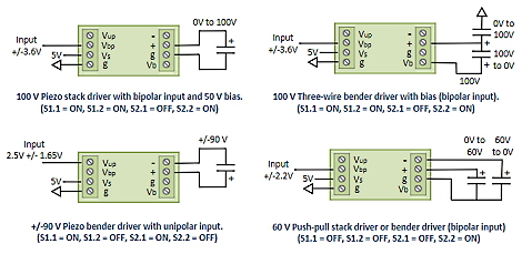
Connection Diagram
Operation
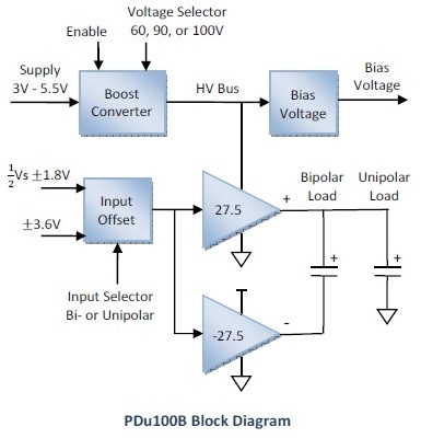
The system block diagram is illustrated below. A boost converter generates a high-voltage rail to supply a pair of complementary amplifiers. A single output can be used to drive a unipolar load up to +100 V or both amplifiers can be used to produce ±100 V.
The input is selectable between a unipolar signal biased at half the supply voltage or a bipolar signal. The amplifier gain is 27.5 so a 3.6 Vp-p input will produce a 100 Vp-p output. Both amplifier channels are biased at half the output range, e.g. 50 V for the 100 V range.
Example Applications
Configuration
The PDu100B can be configured to suit a wide variety of applications. The output voltage range is selected by Switch 1 (S1) as shown below.
| S1.1 | S1.2 | Unipolar Range | Bipolar Range |
|---|---|---|---|
| On | On | 100 V | +/-100 V |
| On | Off | 90 V | +/-90 V |
| Off | On | 70 V | +/-70 V |
| Off | Off | 60 V | +/-60 V |
Output voltage range configuration
The input type can be configured to either unipolar or bipolar with Switch 2 (S2), as shown below.
| Input Type | S2.1 | S2.2 | Input Terminal | Input Range |
|---|---|---|---|---|
| Unipolar | On | Off | Vup | 0.5Vs +/-1.8 V |
| Bipolar | Off | On | Vbp | +/-3.6 V |
Input type configuration
The overall system gain is determined by the configuration of the input and output. The possible combinations are listed below.
| Input Type | Output Type | Gain | Input Range | Output Range |
|---|---|---|---|---|
| Unipolar | Unipolar | 27.5 | 0.5Vs +/-1.8V | 100V |
| Unipolar | Bipolar | 55 | 0.5Vs +/-1.8V | +/-100 V |
| Bipolar | Unipolar | 13.75 | +/-3.6 V | 100V |
| Bipolar | Bipolar | 27.5 | +/-3.6 V | +/-100V |
System gain and voltage range
Both outputs are biased at approximately half the HV bus voltage VHV, e.g. 50 V with a 100 V range. The output voltage equations are listed below.
| Input Type | Output Type | Output Equation |
|---|---|---|
| Unipolar | Unipolar | |
| Unipolar | Bipolar | |
| Bipolar | Unipolar | |
| Bipolar | Bipolar |
System gain and voltage range
The HV bus voltage (and bias output) can be varied by 10% using the trimmer R15. The gain and output voltage ranges can be customized by contacting This email address is being protected from spambots. You need JavaScript enabled to view it..
Offset Voltage
The trim pot R15 adjusts the DC offset voltage, which has a range of +/- 250 mV.
Output Current
The maximum RMS and average DC output current for each voltage range is listed below. The average DC current is the average current flowing in either the positive or negative direction. For a sine wave, the average DC current is related to the RMS current by
![]()
| Voltage Range | RMS Current | Average Current |
|---|---|---|
| 60 V | 89 mA | 40 mA |
| 70 V | 67 mA | 30 mA |
| 90 V | 60 mA | 18 mA |
| 100 V | 33 mA | 15 mA |
Maximum RMS and average DC output current
For periods less than 100 us, output currents of approximately 100 mA are possible. This is useful for achieving small, high-speed step changes in the output voltage.
Power Bandwidth
The power bandwidth is the maximum frequency periodic signal that can be reproduced without distortion. The power bandwidth calculator determines the maximum operating frequency and required power for a given load capacitance. The calculator includes the effects of current limit, slew-rate, and signal bandwidth.
The calculator does not include the time-constant of the peak current limit, and therefore may become inaccurate when the power bandwidth is below 50 Hz. Click Icon to open.
Calculate Power Bandwidth
Signal Bandwidth
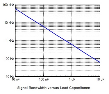
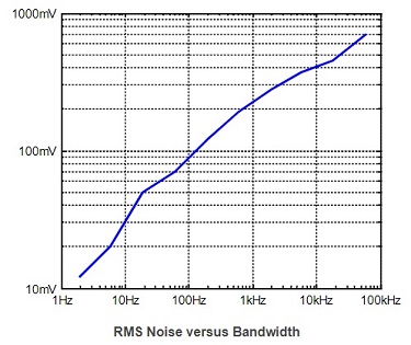
The unloaded small signal bandwidth of the PDu100B is approximately 60 kHz. With a capacitive load, the signal bandwidth is predetermined to be ten times greater than the power bandwidth, that is 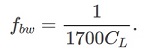 The small signal bandwidth for a range of load capacitances is plotted below and listed in the following table.
Noise
The output voltage of the PDu100B contains switching noise from the boost converter and random noise from the high-voltage amplifier. With a 5 V supply and 100 V output range, the measured noise (Fluke 189) is listed below.
| Load Capacitance (uF) | Signal Bandwidth | Noise (RMS) |
|---|---|---|
| 10 nF | 30 kHz | 550 mV |
| 30 nF | 19 kHz | 450 mV |
| 100 nF | 5.9 kHz | 350 mV |
| 300 nF | 1.9 kHz | 280 mV |
| 1 uF | 590 Hz | 190 mV |
| 3 uF | 190 Hz | 120 mV |
| 10 uF | 59 Hz | 70 mV |
| 30 uF | 19 Hz | 50 mV |
Signal bandwidth and noise
The output voltage noise can be reduced by using an output resistance to reduce the bandwidth. The correct circuit configurations for different applications are illustrated below.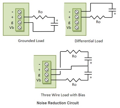
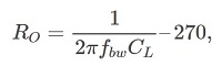
To determine the output resistance required for a particular noise level, the required bandwidth should be selected from Figure 9 below. The correct resistance can then be calculated from
The noise measurements are performed with a static input voltage. When current is drawn from the output, the ripple will increase due to action from the boost converter.
Power Dissapation
With a capacitive load, power dissipation is the product of supply voltage and average current, that is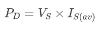
When operating at full power bandwidth, the worst-case power dissipation is approximately 2.5 W. The thermal impedance of the PDu100B from junction to ambient is 30 K/W. Therefore, the maximum temperature rise is approximately 75 degrees C above ambient.
If full-power operation is required at ambient temperatures exceeding 50 degrees C, a 21 mm heat-sink is recommended on the bottom surface. This also requires the connectors to be mounted on the opposite side of the PCB (e.g. Wakefield 624-45ABT3). The order code for a device with unmounted connectors and heat-sink kit is PDu100B-HS.
Enable / Shutdown
The Enable pin can be pulled low to disable the amplifier and reduce the quiescent current to 1 mA. It can be driven by a logic output or an open collector output. The recovery time after a shut-down is 2 ms.
Overload Protection
The PDu100B is protected against over-current and thermal overload. If the temperature exceeds 150 degrees C, the amplifier will be disabled until the temperature reduces.
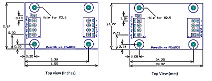
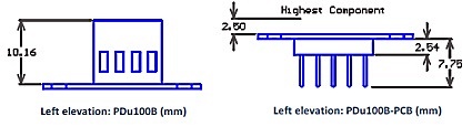
Dimensions
The lateral dimensions are shown in Top views. The mounting holes are designed for an M2.5 threaded spacer. The left elevation of the standard and PCB mounting version (PDu100B-PCB) are shown in the Bottom views. An Altium schematic and footprint library is available for download.