PDu150 Three Channel Ultra-Low Noise 150V
Piezoelectric Drivers
 PDu150 Specifications
 Calculate Power Bandwidth PDu150
Specifications:
| PDu150 Specifications | |||
|---|---|---|---|
| Power Supply | +24 V (+/-10%) | ||
| Output Voltage | -30 V to +150 V | ||
| Peak Current | 100 mA (300 mA single channel) | ||
| RMS Current | 78 mA (235 mA single channel) | ||
| Power Bandwidth | 80 kHz (150 Vp-p) | ||
| Signal Bandwidth | 180 kHz | ||
| Slew Rate | 38 V/us | ||
| Gain | 20 V/V | ||
| Input Impedance | 9.16 kOhm (Input), 3.3 kOhm (Offset) | ||
| Input Offset | +/- 5 mV | ||
| Load | Unlimited | ||
| Output Noise | 26 uV RMS (1 uF load, 0.03 Hz to 1 MHz) | ||
| Protection | Short circuit, over-current, and temperature | ||
| Quiescent Current | 100 mA (10 mA in shutdown) | ||
| Connectors | Screw terminals (AWG 20-30) | ||
| Dimensions | 76 x 40 x 44 mm (L x W x H) | ||
| Environment | 0C to 60C (-40F to 140F) | ||
| Weight | 80 grams | ||
Features
The PDu150 is a complete miniaturized power supply and ultra-low noise driver for up to three 100V, 120V or 150V piezoelectric stack actuators. Output currents up to 100mA per channel are developed at frequencies up to 80 kHz with very low noise. With a capacitive load, the peak-to-peak resolution exceeds one part-per-million or 20-bit, which suits demanding applications in semiconductor machinery, scanning probe microscopy, optics, vibration control, and nanopositioning.
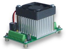
The PDu150 is protected against short-circuit, average current overload, and excessive temperature. Passive cooling is available for low power applications or the integrated fan can be used for power dissipations above 5W. The PDu150 can be mounted with four M2.5 screws. The PCB mounting version (PDu150-PCB) is supplied with headers for direct mounting onto a host motherboard.
Connection Diagram
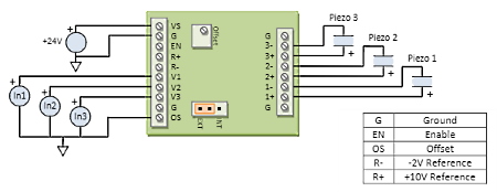
| Pin | Function |
|---|---|
| G | Ground |
| EN | Enable |
| OS | Offset |
| R- | -2V Reference |
| R+ | +10V Reference |
Operation
The amplifiers have differential inputs where the negative input can be connected to an external reference or the internal offset generator. A precision +10V and -2V reference voltage (R+ and R-) are provided to allow external potentiometers to generate the amplifier inputs. The amplifier outputs use a novel low-noise differential architecture that cannot be connected to ground, for example, to the ground lead of an earthed oscilloscope.
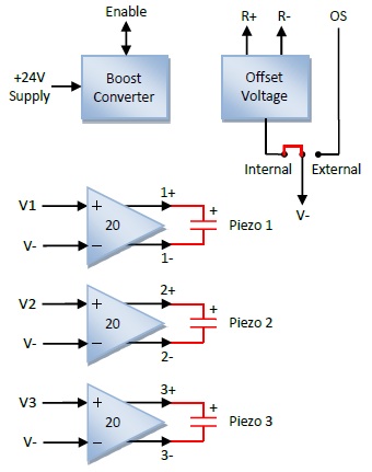
Offset Voltage Configuration
The offset voltage can be set from either the internal potentiometer or by an external source by configuring the jumper LK1 to either “Internal” or “External”. When using the internal offset source, the offset voltage is set by connecting a multimeter across the output and varying the potentiometer until the desired offset is obtained.
In the external offset mode, the offset voltage is determined by the voltage applied to the OS pin. The offset voltage can be set to zero by grounding the OS pin, which is the standard configuration.
Using the Reference Voltages
A precision +10V and -2V reference voltage (R+ and R-) is provided to allow an external potentiometer to generate the amplifier input, as shown below. Multiple potentiometers can be used for multiple channels. The 10uF capacitor reduces the noise bandwidth but is not strictly necessary. The capacitor should preferably be a film type but ceramic is acceptable in most applications.
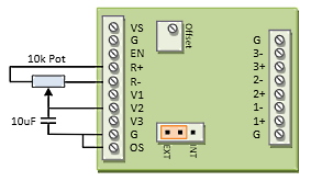
Using the Reference Voltages
Output Current
The peak output current is 100mA per channel or 300mA for three channels in parallel. In addition, the maximum average current is 35mA per amplifier. The average current is useful for calculating the power dissipation and average supply current. For a sine wave, the average positive output current is equal to 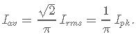
Supply Current
The quiescent power for the amplifier is approximately 2 W or 85 mA. This can be reduced to <10 mA by pulling the Enable pin low with an open collector circuit. If the fan is used, the quiescent power is increased by 0.5W,
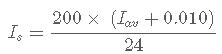
where Iav is the total average output current. The maximum supply current is 0.9A at full power.
Power Bandwidth
The power bandwidth is the maximum frequency periodic signal that can be reproduced without distortion. The calculator determines the maximum operating frequency and required power for a given load capacitance. The calculator includes the effects of current limit, slew-rate, output impedance, and signal bandwidth. The calculator does not include the time-constant of the peak current limit, and may be inaccurate when the power bandwidth is below 100 Hz. (Click Icon)
Calculate Power Bandwidth PDu150
The nominal slew-rate of the PDu150 is 38 V/us. Therefore, the maximum frequency sine-wave is 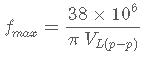
With a capacitive load, the power bandwidth is limited by the output current. The maximum frequency sine wave is 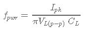 where Ipk is the peak current limit, VL(p?p) is the peak-to-peak output voltage, and CL is the effective load capacitance. Note that when all channels are connected in parallel, the output current and power bandwidth are tripled. In this scenario, the calculator for the PDu150CL will predict performance.
Small Signal Bandwidth
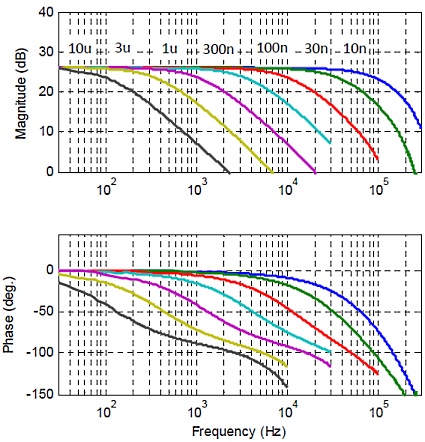
| Load Cap. | Bandwidth |
|---|---|
| No Load | 180 kHz |
| 10 nF | 105 kHz |
| 30 nF | 40 kHz |
| 100 nF | 11 kHz |
| 300 nF | 3.8 kHz |
| 1 uF | 1 kHz |
| 3 uF | 320 Hz |
| 10 uF | 62 Hz |
| 30 uF | 24 Hz |
Small signal bandwidth (-3dB)
Noise
The output noise contains a low frequency component (0.03 Hz to 10 Hz) that is independent of the load capacitance; and a high frequency component (10 Hz to 1 MHz) that is inversely related to the load capacitance. Optimal noise performance is achieved with passive cooling as magnetic fields from the fan can induce mV level interference in the outputs. In low noise applications, where the fan is removed, some external air-flow is required if the power dissipation is above 5W, refer to Heat Dissipation.
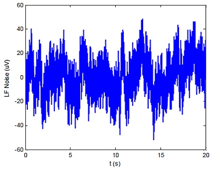
The low frequency noise is measured with an SR560 low-noise amplifier (Gain = 1000), oscilloscope, and Agilent 34461A Voltmeter. The low-frequency noise is plotted below. The RMS value is 15 uV with a peak-to-peak voltage of 100 uV.
The high frequency noise (10 Hz to 1 MHz) is listed in the table on the right versus load capacitance. The total noise from 0.03 Hz to 1 MHz can be found by square summing the RMS values, that is 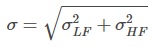
| Load Cap. | HF Noise RMS | Total Noise RMS |
|---|---|---|
| 10 nF | 450 uV | 450 uV |
| 30 nF | 170 uV | 171 uV |
| 100 nF | 60 uV | 62 uV |
| 300 nF | 34 uV | 37 uV |
| 1 uF | 21 uV | 26 uV |
| 3 uF | 16 uV | 23 uV |
| 10 uF | 16 uV | 22 uV |
| 30 uF | 18 uV | 23 uV |
High Frequnecy Noise (10 Hz to 1 MHz) and Total Noise (0.03 Hz to 1 MHz)
Overload Protection / Shutdown
The PDu150 is protected against short-circuit and average current overload. The amplifier can be shutdown manually by pulling the Enable pin low with an open-collector, or open-drain circuit. The Enable pin normally floats at 5V and should not be driven directly.
Heat Dissipation
The heat dissipation is approximately 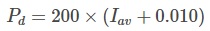
For example, with a sinusoidal output, the power is 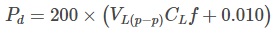
A straight-forward method for measuring heat-dissipation is to measure the supply current with a multimeter during operation. The heat dissipation is equal to the product of DC current and voltage.
In low-noise and low-power applications where it is desirable to remove the fan, natural convection is sufficient if the heat dissipation is less than 5W. If the heat dissipation is above 5W, an external air-flow of 5 CFM is recommended. To avoid interference, external fans should be located further than 80mm from the module.
Safety
This device produces hazardous potentials and should be used by suitably qualified personnel. Do not operate the device when there are exposed conductors. Parts of the circuit may store charge so precautions must also be taken when the device is not powered.
Test Procedures
- See the PDF datasheet for a basic manual test procedure.
- Each PDu150 is extensively tested before shipping using an automated test system. A printed test report is included with each delivered module. An electronic test report, and raw test data can be obtained by contacting PiezoDrive.
Trouble Shooting Notes
- The most common perceived issues with the PDu150 are due to incorrect measurement of the output voltages. The PDu150 output is differential, and the negative outputs (1-, 2-, and 3-) cannot be connected to ground. To measure the output voltage use a battery powered multimeter to measure the voltage between 1+ and 1-, for example.
- To measure the output voltage with an oscilloscope, connect the oscilloscope ground to the PDu150 ground (any G pin), and connect the probe to either the 1+, 2+, or 3+ output. The actual voltage across the load is double what is being measured, which can be accounted for manually, or by doubling the probe sensitivity in the oscilloscope settings, e.g. change the probe sensitivity from 10x to 20x. Do not connect the oscilloscope ground to the 1-, 2-, or 3- terminals.
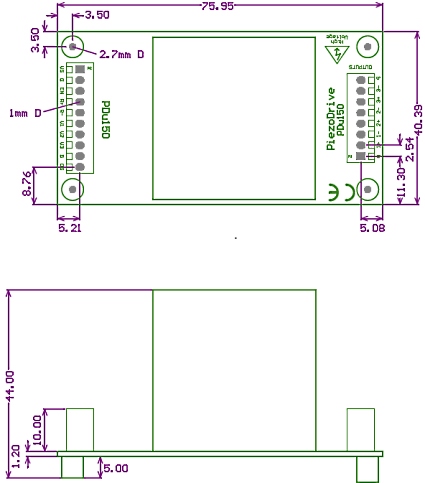
Dimensions
The mounting posts accept M2.5 screws.
The PCB mounting version (PDu150-PCB) is designed to be mounted onto a host motherboard. The only difference is the screw terminals are replaced by headers (Harwin M20-9991045 and M20-9990845) mounted on the bottom side of the module. The recommended PCB hole size for the pins is 1 mm. An Altium schematic and footprint library is available for download.
Click here to download 3D Model
Request a quote for this product by sending an e-mail through "Request for Quote" referencing the part number or by calling us at 814-861-5688 (8:30am to 5:30pm EST).