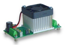
PDu150CL Low Noise 150V Piezo Driver with Strain Gauge Feedback
Piezoelectric Drivers
 PDu150CL Specifications
 Calculate Power Bandwidth PDu150CL
Specifications:
| PDu150CL Specifications | |||
|---|---|---|---|
| Power Supply | +24 V (+/-10% | ||
| Output Voltage | -30 V to +150 V | ||
| Peak Current | 300 mA | ||
| RMS Current | 235 mA | ||
| Power Bandwidth | 80 kHz (150 Vp-p) | ||
| Signal Bandwidth | 180 kHz | ||
| Slew Rate | 38 V/us | ||
| Gain | 20 V/V | ||
| Input Impedance | 10 kOhm (Closed loop mode) | ||
| Input Impedance | 3.05 kOhm (Open loop mode) | ||
| Input Offset | +/- 5 mV | ||
| Load | Unlimited | ||
| Output Noise | 26 uV RMS (1 uF load, 0.03 Hz to 1 MHz) | ||
| Protection | Short circuit, over-current, and temperature | ||
| Quiescent Current | 100 mA (10 mA in shutdown) | ||
| Connectors | Screw terminals (AWG 20-30) | ||
| Dimensions | 89 x 40 x 44 mm (L x W x H) | ||
| Environment | 0C to 60C (32F to 140F) | ||
| Weight | 80 grams | ||
Features
The PDu150CL combines a high-voltage power supply, precision strain conditioning circuit, feedback controller, and ultra-low noise amplifier (26uV RMS) into a package the size of a credit card. It provides all of the necessary functions for high-resolution open-loop or closed-loop control of piezoelectric actuators with or without integrated resistive strain sensors. The PDu150CL develops up to 300mA of output current at frequencies up to 80 kHz with exceptionally low noise. It is suited to demanding applications such as semiconductor machinery, scanning probe microscopy, optics, vibration control, and nanopositioning. The PDu150CL can be purchased as a calibrated pair with an SCL Series Closed-Loop Stack Actuator.
The PDu150CL is protected against short-circuit, average current overload, and excessive temperature. Passive cooling is available for low power applications or the integrated fan can be used when power dissipation is above 5W. The PDu150CL can be mounted with four M2.5 screws or directly to a host motherboard (PDu150CL-PCB).
Connection Diagram
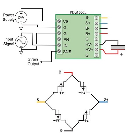
| Pin | Function |
|---|---|
| VS | Power Supply (+24V) |
| G | GRound |
| EN | Enable |
| IN | Signal Input |
| SNS | Sensor Output |
| S-, S+ | Bridge Sensor Connections |
| B-, B+ | Bridge Drive Connections |
| HV-, HV+ | High Voltage Output |
Operation
The PDu150CL can be used in either open-loop or closed-loop modes. In the open-loop mode, the input signal is connected directly to the power amplifier. Note that the amplifier outputs use a novel low-noise differential architecture that cannot be connected to ground, for example, to the ground lead of an earthed oscilloscope.
In the closed-loop mode, the input signal acts as a command signal for the feedback loop. The strain signal is derived from a resistive strain gauge attached to the piezo or structure.
Output Current
The peak output current is 300mA. In addition, the maximum average current is 105mA per amplifier. The average current is useful for calculating the power dissipation and average supply current. For a sine wave, the average positive output current is equal to 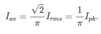
Supply Current
The quiescent power for the amplifier is approximately 2 W or 85 mA. This can be reduced to <10 mA by pulling the Enable pin low with an open collector circuit. If the fan is used, the quiescent power is increased by 0.5W,
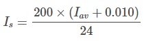
where Iav is the total average output current. The maximum supply current is 0.9A at full power.
Power Bandwidth
The calculator below plots the maximum peak-to-peak output voltage versus the capacitive load and frequency.
Calculate Power Bandwidth PDu150CL
The nominal slew-rate of the PDu150 is 38 V/us. Therefore, the maximum frequency sine-wave is 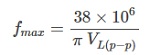 Therefore, the power bandwidth for a 150 Vp-p sine-wave is 80 kHz.
With a capacitive load, the power bandwidth is limited by the output current. The maximum frequency sine wave is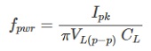 where Ipk is the peak current limit, VL(p-p) is the peak-to-peak output voltage, and CL is the effective load capacitance.
Small Signal Bandwidth
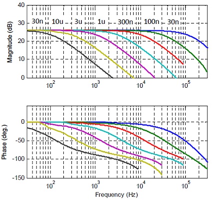
| Load Cap. | Bandwidth |
|---|---|
| No Load | 180 kHz |
| 30 nF | 120 kHz |
| 100 nF | 34 kHz |
| 300 nF | 11 kHz |
| 1 uF | 3.2 kHz |
| 3 uF | 980 Hz |
| 10 uF | 190 Hz |
| 30 uF | 73 Hz |
Power Amplifier Noise
The output noise contains a low frequency component (0.03 Hz to 10 Hz) that is independent of the load capacitance; and a high frequency component (10 Hz to 1 MHz) that is inversely related to the load capacitance. Optimal noise performance is achieved with passive cooling as magnetic fields from the fan can induce mV level interference in the outputs. In low noise applications, where the fan is removed, some external air-flow is required if the power dissipation is above 5W, refer to Heat Dissipation
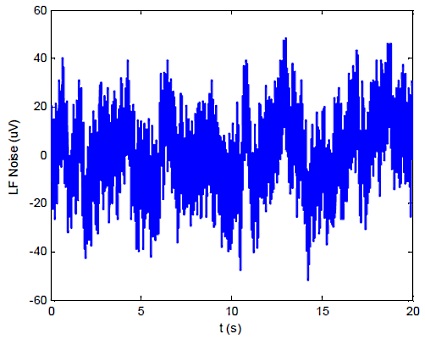
The noise is measured with an SR560 low-noise amplifier (Gain = 1000), oscilloscope, and Agilent 34461A Voltmeter. The low-frequency noise is plotted below. The RMS value is 15 uV with a peak-to-peak voltage of 100 uV.
The high frequency noise (10 Hz to 1 MHz) is listed in the table below versus load capacitance. The total noise from 0.03 Hz to 1 MHz can be found by square summing the RMS values, that is 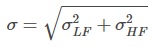 .
.
| Load Cap. | HF Noise RMS | Total Noise RMS |
|---|---|---|
| 10 nF | 450 uV | 450 uV |
| 30 nF | 170 uV | 171 uV |
| 100 nF | 60 uV | 62 uV |
| 300 nF | 34 uV | 37 uV |
| 1 uF | 21 uV | 26 uV |
| 3 uF | 16 uV | 23 uV |
| 10 uF | 16 uV | 22 uV |
| 30 uF | 18 uV | 23 uV |
Strain Sensor Specifications
| Strain Sensor Specifications | ||
|---|---|---|
| Bridge Excitation | 5V (Differential) | |
| Sensor Resistance | 350 Ohm to 1000 Ohm | |
| Sensor Configuration | Single, Half, or Full Bridge | |
| Bridge Balance Range | +/-6 mV | |
| Gain Range | 200 to 3000 | |
| Offset Range | +/-6 mV | |
| Bandwidth | 10 kHz | |
| Input Noise Voltage | 3 uV RMS (0.1 Hz to 100 Hz) | |
Sensor Connection
The PDu150CL is compatible with single element strain sensors, half-bridges, and full-bridge sensor arrangements. The advantages of these different arrangements and the recommended methods of connection are described in the following. Suitable strain sensors are available from many suppliers, including www.omega.com. The PDu150CL can be purchased as a calibrated pair with an SCL Series Closed-Loop Stack Actuator.
Single Element Strain Gauge
Single element strain sensors can be useful in applications where the temperature is stable or simplicity is a priority. As shown below, the recommended configuration requires three dummy resistors (R) equal in resistance to the strain gauge. The best temperature stability is achieved when the dummy resistors have the same temperature coefficient as the strain gauge and are thermally connected to the strain gauge.
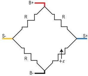
Half Bridge Strain Sensor
A half bridge arrangement with a 90 degree rosette sensor provides good immunity to temperature variation and approximately 30% better resolution than a single element. The recommended configuration requires two dummy resistors (R) that are equal in value to the strain gauge resistance.
The strain element aligned to the piezo expansion is denoted by (+ε) and the 90 degree element is denoted(-νε). This convention is adopted since a positive strain in the piezo +ε causes a negative resistance change in the 90 degree element due to Poisson's ratio (ν).
Full Bridge Strain Sensor
A full-bridge arrangement constructed from two 90 degree rosette sensors provides good immunity to temperature variation, the best linearity, and twice the resolution of a half bridge; however, this configuration also requires more wiring. The PDu150CL can be purchased as a calibrated pair with an SCL Series Closed-Loop Stack Actuator.
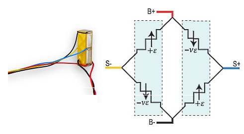
The strain element aligned to the piezo expansion is denoted by (+ε) and the 90 degree element is denoted(-νε). This convention is adopted since a positive strain in the piezo +ε causes a negative resistance change in the 90 degree element due to Poisson's ratio (ν).
Sensor Noise and Resolution
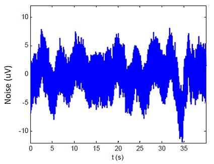
Since the sensor noise is filtered by the complementary sensitivity function of the control loop, the bandwidth of interest is typically 0.1Hz to 100Hz. The upper frequency limit has little effect since the majority of noise in this bandwidth is due to low-frequency noise from the on-board references and primary gain stage. With a bridge resistance of 350 Ohms, the total input referred noise voltage is plotted below, the RMS value is 3uV with a peak-to-peak voltage of 20uV.
The sensor noise can be used to estimate the sensor resolution. The induced voltage for a two-varying element full bridge is [1, 2]
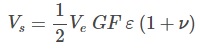
Where Ve is the excitation voltage (5V), GF is the gauge factor (typically ~2), ε is the strain, and ν is the Poisson's ratio (0.34 for PZT5H). For a full-scale strain of 0.1%, the expected bridge voltage is 6.7 mV. Therefore, the expected RMS resolution is

Sensor Calibration Procedure
The following procedures are required to calibrate the bridge conditioning circuit and should be performed with the sensor and piezo connected to the PDu150CL.
Balance the Bridge
Small mismatches in the bridge resistances can be accounted for by the Bridge Balance pot. This step optimizes the temperature sensitivity of the bridge circuit.
- Place the PDu150CL in Open-Loop mode and apply 0V or a short-circuit to the input terminals.
- Connect a voltmeter between the S- and S+ terminals (without disconnecting the bridge).
- Tune the Bridge Balance pot until the measured voltage is zero.
Set the Sensitivity and Offset
This step calibrates the sensor so that a 0V to 150V signal applied to the piezo produces a 0V to 10V strain signal.
- Turn the Sensor Gain pot fully anti-clockwise, (10 turns).
- Ensure the PDu150CL is in Open-Loop mode and apply 0V or a short-circuit to the input terminals.
- Monitor the SNS terminal and tune the Sensor Offset pot until the voltage is zero.
- Apply 7.5V to the input terminal to generate 150V across the piezo.
- Monitor the SNS terminal and tune the Sensor Gain pot until the voltage is +10V.
Variations
Many variations of the above procedure are possible. Some useful options are listed below.
The offset and gain can be tuned simultaneously by applying a 5-Hz sine wave to the input terminals with a range of 0V to 7.5V, which results in 0V to 150V across the piezo. Monitor the SNS terminal with an oscilloscope and tune the Sensor Offset and Sensor Gain pots until the measured sine-wave is between 0V and 10V.
Rather than calibrating the sensor to +10V at full scale, another voltage such as +5V may be more desirable.
If negative voltages across the piezo are acceptable, it is convenient to calibrate the full piezo voltage range, e.g. -30V to +150V, to a SNS voltage of 0V to +10V. This requires an input of -1.5V to +7.5V during calibration, rather than 0V to +7.5V.
For stack actuators with different voltage ratings, the calibration input signal should be chosen accordingly. For example, a suitable calibration input for a piezo with a voltage rating -20V to +100V would be -1V to +5V.
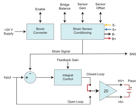
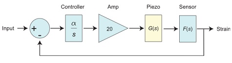
Closed-Loop Operation
Once the sensor is calibrated, the PDu150CL can be placed in closed-loop mode. The structure of the closed-loop system is illustrated below.
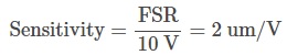
The closed-loop sensitivity is defined by the sensitivity of the strain sensor. For example, if the piezo has a full-scale range (FSR) of 20 um and the strain sensor is calibrated for 0V to 10V, the closed loop sensitivity is
Calibrating the Feedback Gain
The feedback gain defines the closed-loop bandwidth and settling time of the system. It is usually advantageous to choose the lowest satisfactory feedback gain to avoid unnecessary sensor noise. A simple calibration procedure is described in the following:
- Turn the Feedback Gain pot fully anti-clockwise (10 turns).
- Place the PDu150CL in closed-loop mode and apply a 1Vp-p triangle wave with a 5V offset to the input terminal. If the sensor was calibrated with a full scale range other than 10V, use an offset voltage equal to mid-range.
- Monitor the input signal and SNS terminal with an oscilloscope and increase the feedback gain until the point where overshoot begins to occur.
For applications that do not require high-speed tracking, the above procedure is not required. The minimum feedback gain is suitable. To achieve a specific -3dB bandwidth, replace the triangle wave with a sine-wave and tune the feedback gain until the amplitude of the SNS signal is 0.7 Vp-p.
Headroom
When the full-scale range of the sensor is calibrated to the full-scale range of the piezo, some consideration for ‘headroom’ is required. To allow the control loop to compensate for effects such as thermal drift and creep, the input signal is typically restricted to a range of 10% to 90% so that the control-loop can utilize the remaining 10% at the lower and upper extremes. For example, a system with a full-scale range of 0V to 10V, would have a practical closed-loop input range of 1V to 9V.
An alternative to the above approach is to account for headroom during calibration. For example, rather than using the full scale range for calibration, e.g. -30V to +150V, a smaller range can be chosen, e.g. -15V to +130V. By using this method, the resulting closed-loop input range will be 0V to 10V, which may be more desirable than 1V to 9V.
Example Application
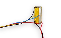
In this example, the piezoelectric stack actuator pictured below (SCL050518) is operated in closed-loop. The actuator develops a displacement of 20um at 150V and utilizes a full-bridge strain sensor constructed from two 90 degree rosettes.
The PDu150CL was calibrated so that an applied voltage of 0V to 150V corresponds to a strain signal of 0V to 10V. The feedback gain was then chosen to achieve good tracking performance with a 10-Hz full-range triangle wave, as shown below.
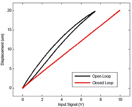
The open- and closed-loop responses to a full-range 1-Hz sine-wave input are plotted below. Excellent compensation of hysteresis can be observed.
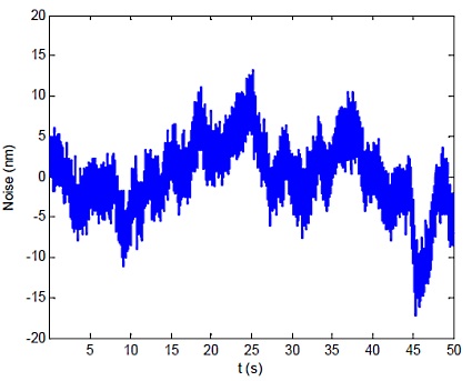
Before evaluating the total positioning noise, the feedback gain is adjusted to provide a closed-loop bandwidth of precisely 20 Hz by applying a 20-Hz sine-wave and varying the feedback gain until the amplitude response is -3dB. This allows a direct comparison to other methods with an identical bandwidth.
The total positioning noise due to the amplifier, sensor, and feedback controller can then be quantified by measuring the differential output voltage of the power amplifier with a zero volt input [3].
The differential output voltage was measured using an SR560 low-noise amplifier with a gain of 10 and a passband of 0.03 Hz to 1 MHz. The resulting voltage was scaled by the sensitivity of the piezo (20um/150V) and is plotted below. The RMS value is 8.8 nm with a peak-to-peak value of 60 nm over 50 seconds. This represents an RMS resolution of

This value agrees with the predicted resolution in “Sensor Noise and Resolution”.
Overload Protection / Shutdown
The PDu150 is protected against short-circuit and average current overload.
The amplifier can be shutdown manually by pulling the Enable pin low with an open-collector, or open-drain circuit. The Enable pin normally floats at 5V and should not be driven directly.
Heat Dissipation
The heat dissipation is approximately 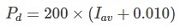
For example, with a sinusoidal output, the power is 
A straight-forward method for measuring heat-dissipation is to measure the supply current with a multimeter during operation. The heat dissipation is equal to the product of DC current and voltage.
In low-noise and low-power applications where it is desirable to remove the fan, natural convection is sufficient if the heat dissipation is less than 5W. If the heat dissipation is above 5W, an external air-flow of 5 CFM is recommended. To avoid interference, external fans should be located further than 80mm from the module.
Safety
This device produces hazardous potentials and should be used by suitably qualified personnel. Do not operate the device when there are exposed conductors. Parts of the circuit may store charge so precautions must also be taken when the device is not powered.
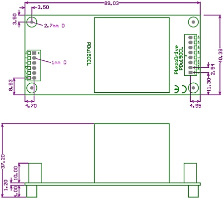
Dimensions
The mounting posts accept M2.5 screws. The PCB mounting version (PDu150CL-PCB) is designed to be mounted onto a host motherboard. The only difference is the screw terminals are replaced by headers (Harwin M20-9990545 and M20-9990845) mounted on the bottom side of the module. The recommended PCB hole size for the pins is 1 mm. An Altium schematic and footprint library is available for download.
Request a quote for this product by sending an e-mail through "Request for Quote" referencing the part number or by calling us at 814-861-5688 (8:30am to 5:30pm EST).
Click here to download 3D model
Previous Versions
| Hardware Version | Manufactured | Manual |
|---|---|---|
| V4 | 2016-2017 | Download Datasheet |
References
- A Review of Nanometer Resolution Position Sensors: Operation and Performance; A. J. Fleming; Sensors and Actuators A: Physical; 2013, 190, 106-126
- Design, Modeling and Control of Nanopositioning Systems; A. J. Fleming & K. K. Leang; Springer, 2014
- Measuring and Predicting Resolution in Nanopositioning Systems; A. J. Fleming; Mechatronics; 2014, 24, 605-618