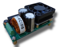
MX200 High Performance Voltage Amplifier
Piezoelectric Drivers
 MX200 Specifications
 Calculate Power Bandwidth MX200
Specifications:
| MX200 Specifications | |||
|---|---|---|---|
| Power Supply | 24 V (18V to 36V ) | ||
| Voltage Range | +100 V, +150 V, +200 V | ||
| RMS Current | 550 mA, 330 mA, 220 mA | ||
| Peak Current | 1 Amp | ||
| Power Bandwidth | 106 kHz (180 Vp-p) | ||
| Signal Bandwidth | 200 kHz (100nF Load) | ||
| Slew Rate | 60 V/us | ||
| Gain | 20 V/V | ||
| Input Impedance | 33 kOhm (In+), 1.6 kOhm (In-) | ||
| Input Offset | +/-5 mV | ||
| Load | Unlimited | ||
| Output Noise | <1 mV RMS (1 uF Load) | ||
| Protection | Over-current and Under-voltage | ||
| Quiescent Current | 0.3 A (30 mA in shutdown) | ||
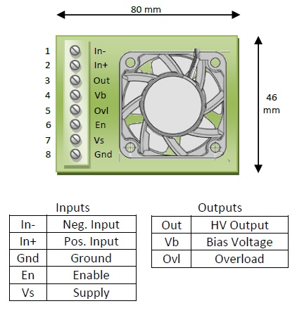
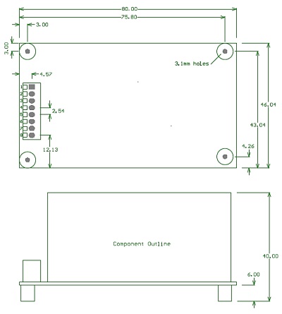
| Dimensions | 80 x 46 x 40 mm (L x W x H) | ||
| Environment | -40 to 60 Celsius (-40 to 140 F) | ||
| Weight | 95 gram | ||
Features
The MX200 is a complete power supply and high-performance linear amplifier module for driving piezoelectric actuators. The MX200 can drive stack actuators; standard piezoelectric actuators; two wire benders; and three-wire piezoelectric benders requiring a bias voltage. Output currents of up to 1 Amp are developed at frequencies up to 100 kHz.
The MX200 is protected against short-circuit, average current overload, and supply under-voltage. The MX200 can be used as a stand-alone module or mounted to a base with four M3 screws. The PCB mounting version (MX200-PCB) is supplied with headers for direct mounting onto a host motherboard.
Compatible Actuators
| Compatible Actuators | |||
|---|---|---|---|
| Stack Actuators | 60V, 100V, 120V, 150V, 200V | ||
| Plates and Tubes | up to +/- 200V | ||
| Three Wire Benders | 0 to 200V with 200V bias | ||
| Three Wire Benders | +/-100V with +/-100V bias | ||
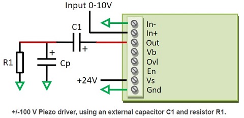
Connection Diagram
Operation
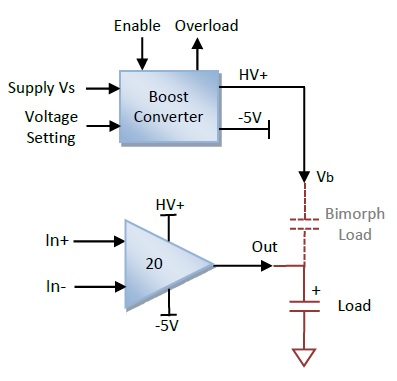
A boost converter generates the high voltage supply and negative rail. The output voltage range can be set to either +100V, +150V, or +200V. Configuration options are discussed in the following section. The high-voltage amplifier has differential inputs with a gain of 20 and an input voltage range of 10 V. The negative input can be connected to ground or to a differential source. It should not be left floating. The load is connected between the output and ground. The bias voltage output is for three wire bimorph bender actuators.
Configuration
The output voltage range can be set to either +100V, +150V or +200V using the two jumpers LK1 and LK2. Greater output current is available in the lower voltage ranges. Incorrect jumper combinations will damage the amplifier.
| Voltage Range | Peak Current | RMS Current | Average Current | LK1 | LK2 |
|---|---|---|---|---|---|
| 100 V | 1 Amp | 550 mA | 250 mA | A | Out |
| 150V | 1 Amp | 330 mA | 150 mA | B | B |
| 200V | 1 Amp | 220 mA | 100 mA | Out | A |
Output Current
The maximum continuous RMS current is dependent on the voltage range, as described in Table 1. The average positive output current is also useful for calculating power dissipation and the average supply current. For a sine wave, the average positive output current is equal to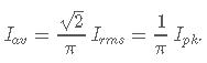
The peak current limit for all voltage ranges is +/-1A, which can be supplied for up to 5ms. This is useful in pulse applications where a fast rise-time is required.
Supply Current
The quiescent power for the amplifier and fan is approximately 8 W. Therefore, the quiescent supply current at 24 V is 0.3 A. This can be reduced to 30 mA by applying a logic zero to the Enable pin. The supply current is related to the average positive output current by
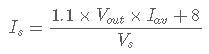
where Vout is the output voltage range, and Iav is the average output current. Therefore, the maximum supply current is 1.25 A with a 24 V supply at the full rated power (Iav=100 mA).
The power supply must be sufficient for the amplifier, a rating of at least 1.5 Amps is recommended. Note that when power is first applied or when the amplifier is enabled, full current will be required for a brief period to charge the storage capacitors.
Application Circuits
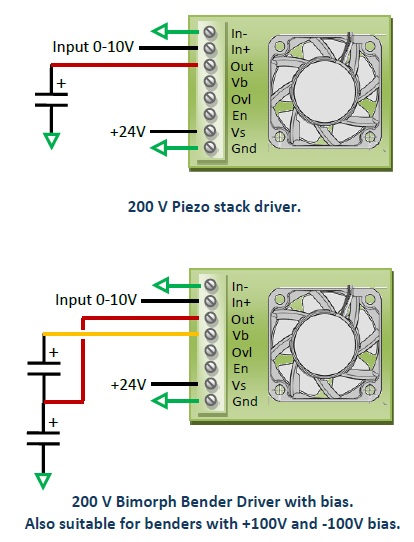
Bias Output for Piezo Bimorphs
The bias output (Vb) provides a fixed voltage for driving three-wire piezoelectric benders. The bias voltage is approximately 5V above the selected voltage range. The effective capacitance when using bimorph actuators is the sum of both layers.
Actuators that require a symmetrical bias voltage, e.g. +/-100 V can also be driven since this configuration is electrically identical to the unipolar configuration, e.g. 0V to 200V.
Power Bandwidth
The online power bandwidth calculator estimates the highest achievable frequency with a capacitive load impedance. The calculator considers the current limit, slew-rate, output impedance, and small-signal bandwidth.
Calculate Power Bandwidth
The maximum frequency with no load is limited by the slew-rate of 60 V/us. That is, 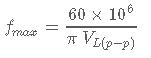
With a capacitive load, the power bandwidth is limited by the output current. The maximum frequency sine wave is 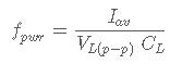 where Iav is the average current limit (100 mA for the 200V range), VL(p-p) is the peak-to-peak output voltage, and CL is the effective load capacitance.
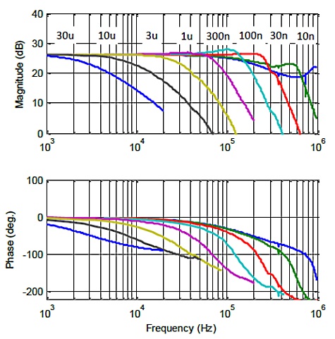
Small Signal Bandwidth
| Load Cap. | Bandwidth |
|---|---|
| 10 nF | 180 kHz |
| 30 nF | 283 kHz |
| 100 nF | 275 kHz |
| 300 nF | 160 kHz |
| 1 uF | 78 kHz |
| 3 uF | 30 kHz |
| 10 uF | 8.3 kHz |
| 30 uF | 3.0 kHz |
Noise
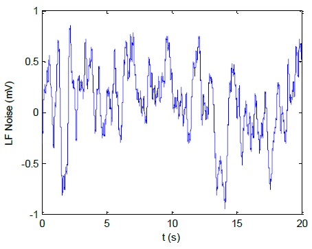
The output noise contains a low frequency component (0.03 Hz to 10 Hz) that is independent of the load capacitance; and a high frequency component (10 Hz to 1 MHz) that is inversely related to the load capacitance. Note that many manufacturers quote only the AC noise measured by a multimeter (20 Hz to 100 kHz) which is usually a gross underestimate.
The noise is measured with an SR560 low-noise amplifier (Gain = 1000), oscilloscope, and Agilent 34461A Voltmeter. The low-frequency noise is plotted below. The RMS value is 360 uV with a peak-to-peak voltage of 1.8 mV.
The high frequency noise (10 Hz to 1 MHz) is listed in the table below versus load capacitance. The total noise from 0.03 Hz to 1 MHz can be found by square summing the RMS values, that is 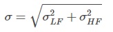 .
.
| Load Cap. | HF Noise RMS | Total Noise RMS |
|---|---|---|
| 10 nF | 1.5 mV | 1.5 mV |
| 30 nF | 2.6 mV | 2.6 mV |
| 100 nF | 3.5 mV | 3.5 mV |
| 300 nF | 1.2 mV | 1.2 mV |
| 1 uF | 306 uV | 470 uV |
| 3 uF | 129 uV | 380 uV |
| 10 uF | 100 uV | 370 uV |
| 30 uF | 120 uV | 380 uV |
The majority of high-frequency noise is due to ripple from the boost converter (at 170 kHz). In ultra-low noise applications, the output bandwidth can be restricted to 10 kHz which reduces the noise to less than 100 uV RMS in the 10 Hz to 1 MHz frequency range. This can be achieved with the RLC filter shown below.
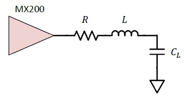
The required inductance and resistance is 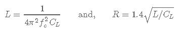 where fc is the cut-off frequency (10 kHz) and CL is the load capacitance. The inductor should be rated for at least 1 A with a self-resonance frequency of greater than 1 MHz. A first-order resistive filter can also be effective, although it must be rated for the expected RMS current. The required value is
Optimal Noise Performance
The MX200 has an internal boost converter which results in approximately 1A current ripple between Pin 7 and Pin 8. To minimize ground noise due to the supply impedance and wiring inductance, use twisted pair wiring. Aluminium Polymer capacitors are recommended between pins 7 and 8 (35V, 1000uF to 10,000uF). The total capacitance should be less than half the maximum capacitance specification of your 24V supply.
The MX200 has a differential input to minimize the effect of ground voltage disturbances. The signal source should be connected by a twisted pair cable to Pin 1 and Pin 2, preferably with a grounded shield. For the standard non-inverting configuration, the signal source ground should be connected to Pin 1 at the signal source.
If noise is a critical concern, the output filter described above should be considered.
When measuring output noise, ensure the probe ground and signal leads are connected directly connected to the load. Do not use remote ground connections.
Overload Protection / Shutdown
The MX200 is protected against short-circuit and average current overload. The module is also disabled when the input supply voltage is less than 12 V. Current overload conditions are signaled by +5 V on the Overload pin.
The amplifier can be shutdown manually by pulling the Enable pin low with an open-collector, or open-drain circuit. The Enable pin normally floats at 6.2V and should not be driven directly.
Safety
This device produces hazardous potentials and should be used by suitably qualified personnel. Do not operate the device when there are exposed conductors.Parts of the circuit may store charge so precautions must also be taken when the device is not powered.
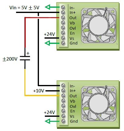
Bridge Configuration
The output voltage range can be doubled to +/-200 V by driving the load in a bridged configuration as shown below. In this configuration, the output voltage is 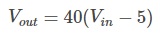
That is, a 0V to 10V input produces +/-200V at the load. Zero volts across the load occurs when the input voltage is +5V. However, note that the absolute voltage of each terminal is still +100V. The power bandwidth for this configuration can be calculated by considering only one amplifier and doubling the effective capacitance.
Bipolar Output Voltage
Bipolar output voltages can be achieved by adding an external AC coupling capacitor, as shown in the diagram below. This approach creates a high-pass filter with a cut-off frequency of 1 Hz. That is, frequencies below 1 Hz will be strongly attenuated.
Up to +/-100V can be obtained using the 200V range, or +/-75V using the 150V range, or +/-50V using the 100V range.
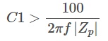
C1 should be rated for at least the full output voltage of the amplifier. For example, to achieve +/-100V using the 200V configuration, a 250V rated capacitor is required. The capacitance of C1 should be large enough to ensure the series voltage drop is less than 1% of the output voltage. Film capacitors are preferred but electrolytic capacitors are also suitable.
If the load is a piezo or capacitor, C > 100 x Cp
If the load is not capacitive at the operating frequency, the impedance of C1 should be less than 1% of the load impedance , that is,
The resistor R1 sets the AC coupling frequency , which is recommended to be 1 Hz. The value of R1 is
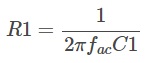
The power rating of R1 should be greater than  , where V2RMS is the RMS voltage across the load.
Dimensions
The mounting posts accept M3 screws. For the PCB mounting version (MX200-PCB), an Altium schematic and footprint library is available for download.
Click here to download 3D model.
Request a quote for this product by sending an e-mail through "Request for Quote" referencing the part number or by calling us at 814-861-5688 (8:30am to 5:30pm EST).